Description

The accuracy is as high as sub-nanometer level, and the online detection is as fast as 1 second
Roughness・steps・contour・3D topography・SEM-like effect
Applications for Wide Range of Industries
1. The ability to accurately capture ultra-high-precision microscopic 3D topography
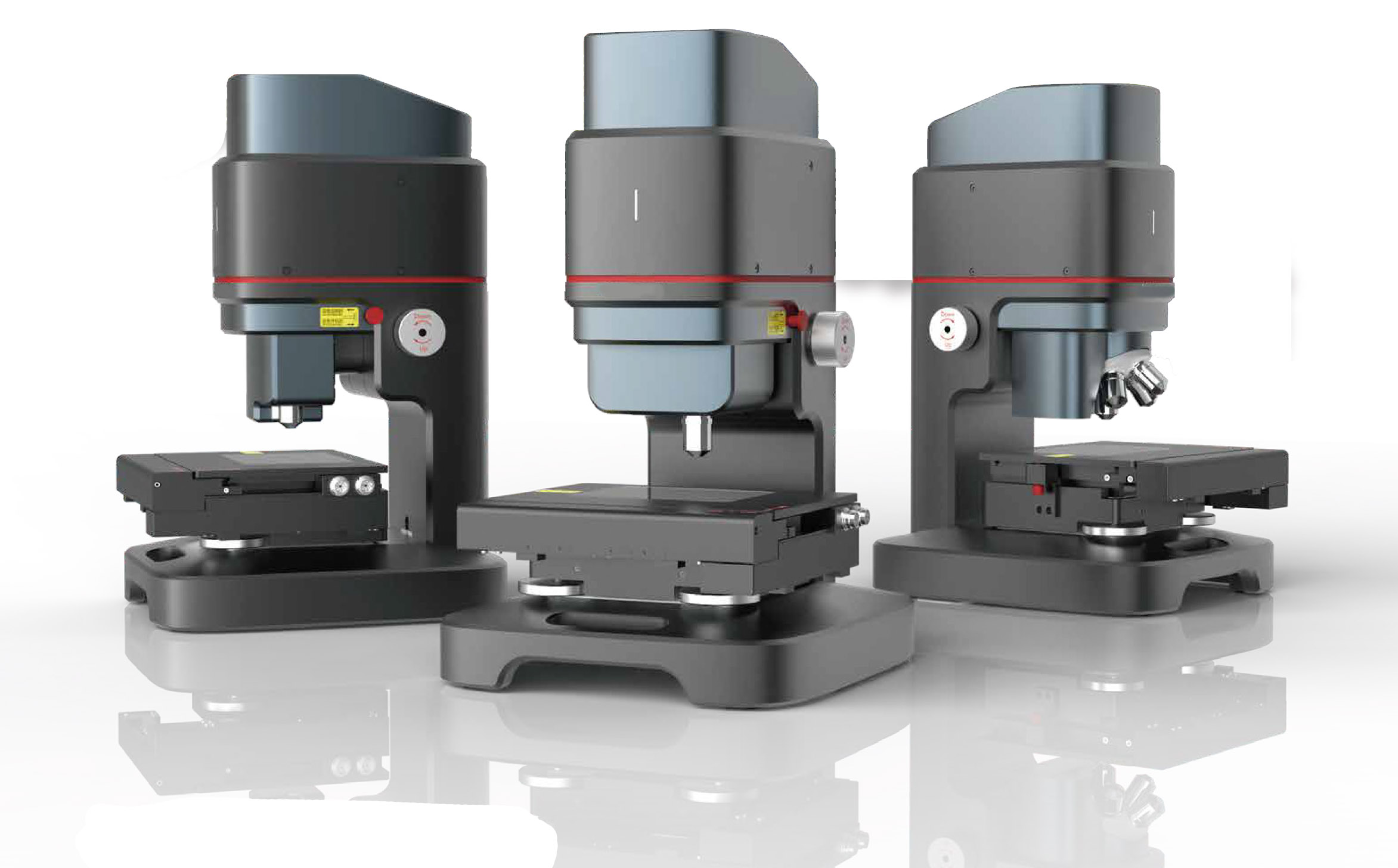
AM-200 can be used to measure the surface of various precision devices and materials at sub-nanometer level, and obtain the surface 3D topography in the form of “surface” The 3D morphology is processed and analyzed by special software, and the highest RMS repeatability can reach 0.002nm
2. Ultra-high speed greatly improves measurement efficiency and can be used in automated production lines
AT0-200 is equipped with large-scale and high-speed nano-piezoelectric ceramic devices, with a maximum scanning speed of 400μm/s, 3200Hz and the industry’s first SST+GAT algorithm, which can instantly complete the acquisition of up to 5 million point clouds
3. Large field of view and high precision Large field of view and large-scale measurement
Principle of white light interferometry phase metrology by light interferometry The detection accuracy of <1nm can be obtained under any magnification
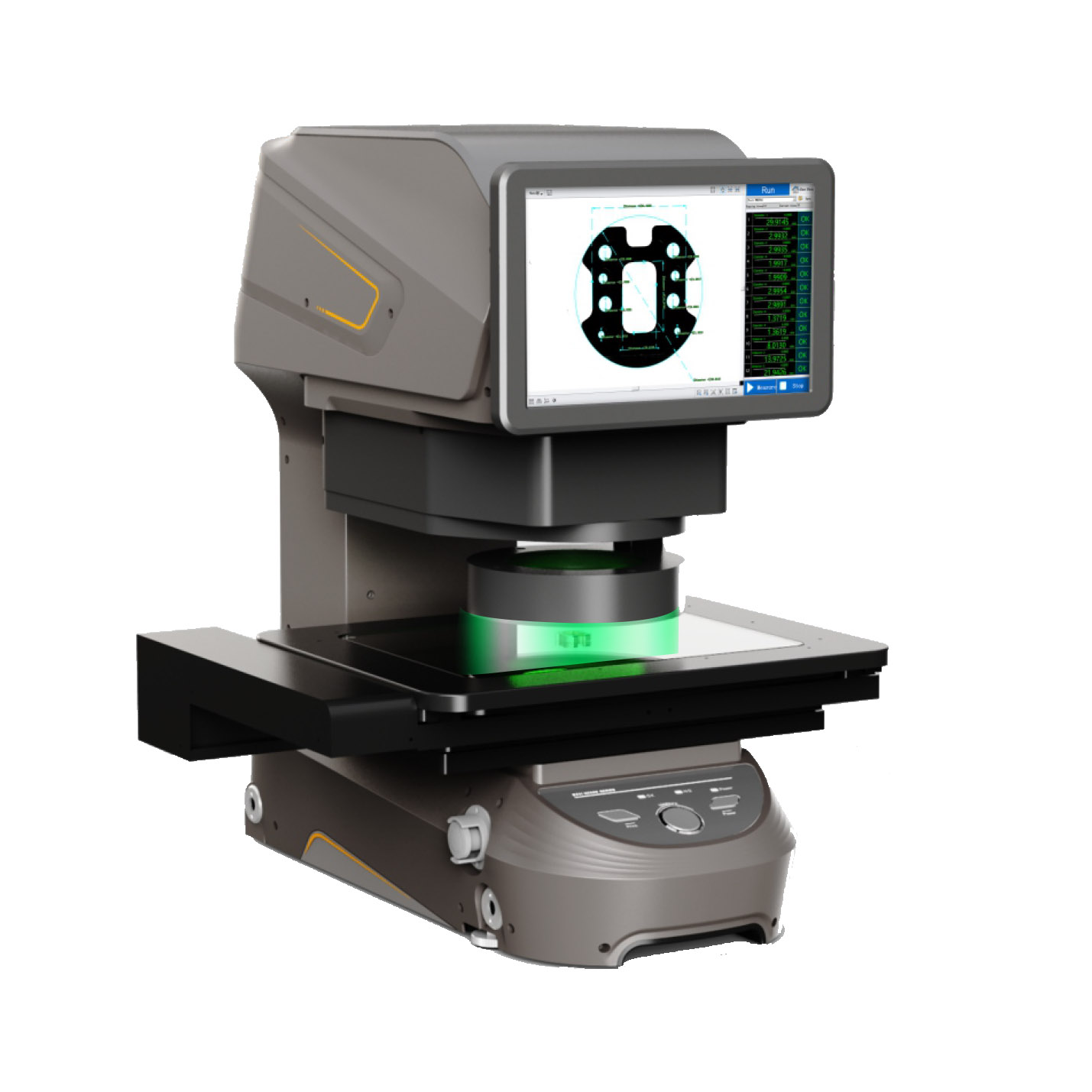
4. Abundant measurement tools to easily cope with various industry applications
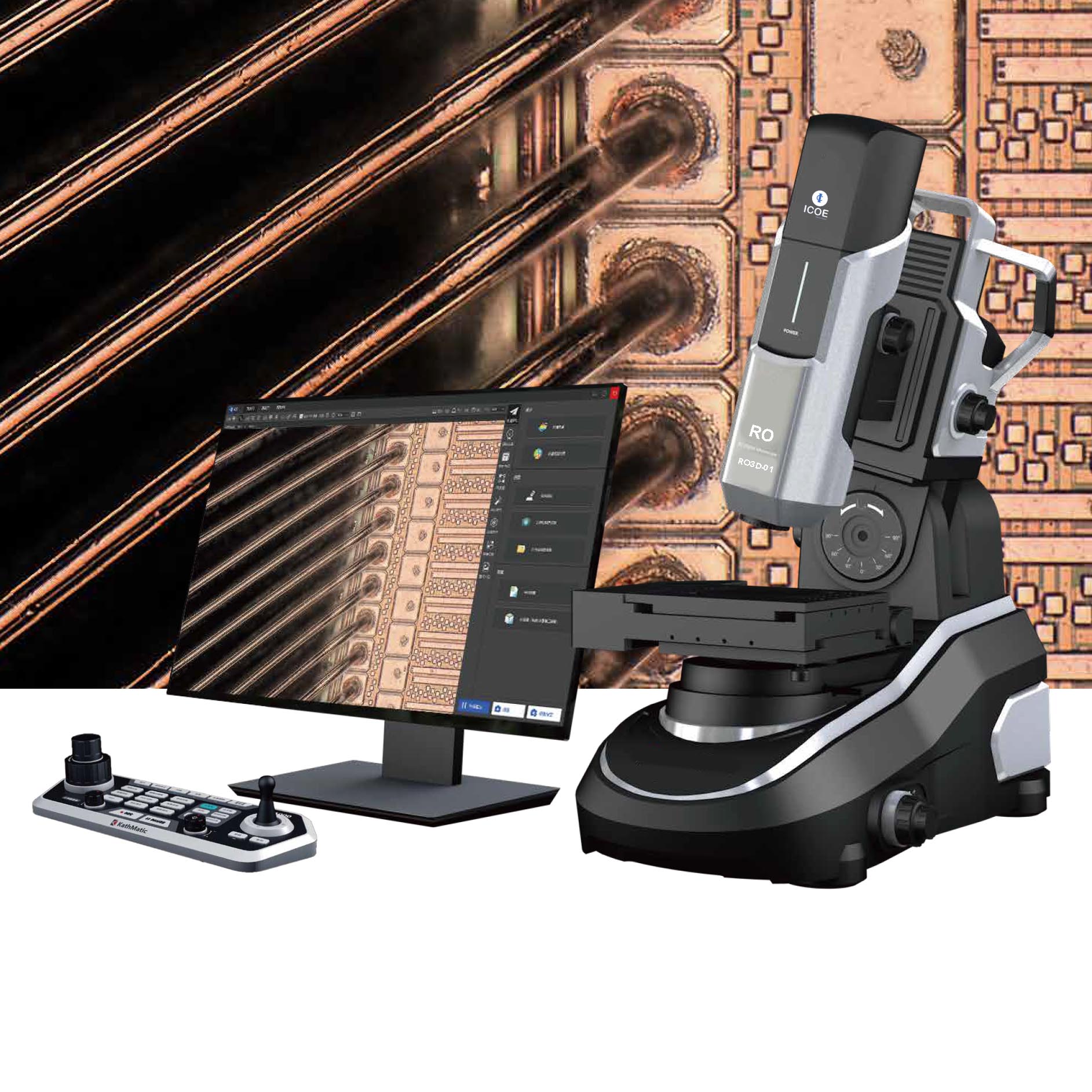
Covers common international standard measurement tools on the market, and can analyze 3D data efficiently and easily


